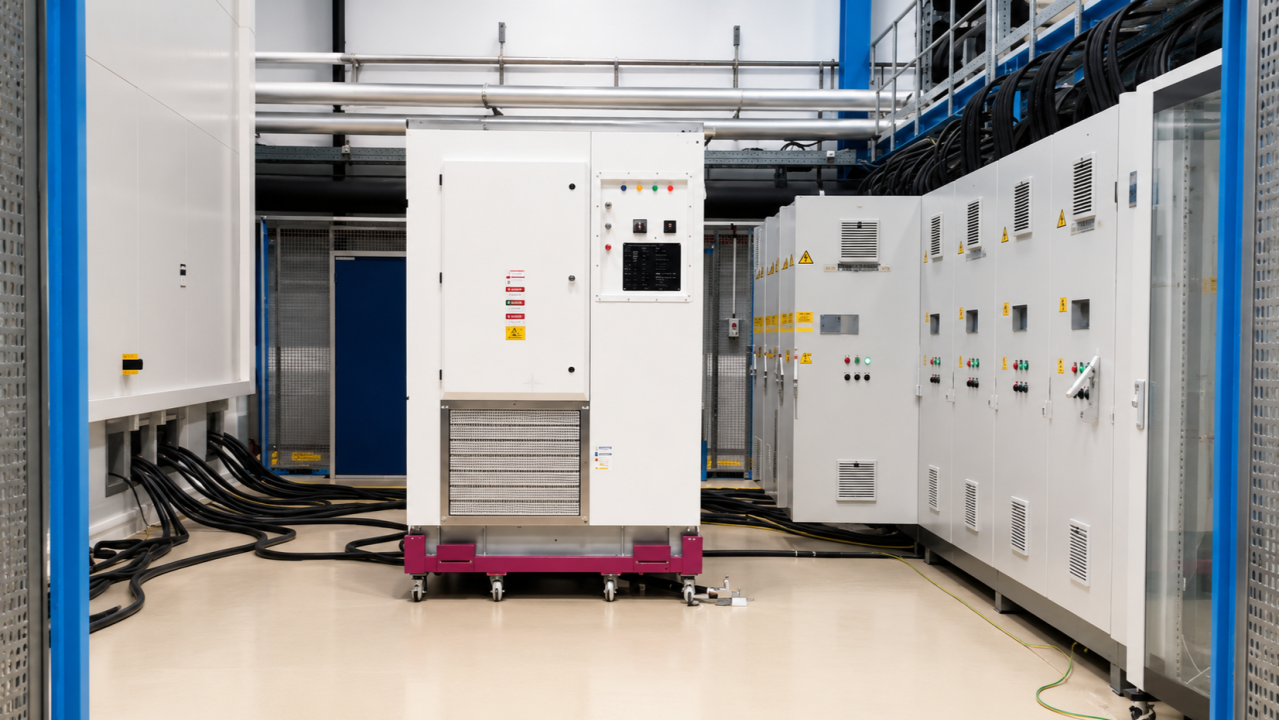
The global energy transition is placing unprecedented stress on conventional power infrastructure. Battery Energy Storage Systems (BESS) have emerged as a cornerstone of grid modernization — enabling peak shaving, frequency regulation, renewable integration, and energy arbitrage. Yet the traditional Low-Frequency Transformer (LFT) at the heart of most BESS architectures imposes fundamental limits: it is bulky, oil-insulated, cannot regulate power flow, and provides no native DC port for storage integration. The Solid-State Transformer (SST), also called a Power Electronic Transformer (PET), is being actively developed to overcome these limitations — offering bidirectional power flow control, multi-port DC integration, active power quality management, and a dramatically reduced physical footprint.

The global SST market, valued at approximately USD 172–194 million in 2024–2025, is projected to grow at a CAGR of 13–32% depending on the analyst, potentially reaching USD 500–936 million by 2030–2032. While the opportunity is large, commercialization faces deep-rooted technical, economic, and regulatory barriers. This article provides a detailed treatment of SST fundamentals, the specific difficulties encountered in BESS integration, the structural barriers to mainstream adoption, and the key industry players shaping this space.
Fundamentals of Solid-State Transformers
What is an SST?
A Solid-State Transformer is an advanced power conversion device that replaces the conventional iron-core, line-frequency (50/60 Hz) transformer with semiconductor-based power electronics operating at medium-to-high frequencies (tens of kilohertz to hundreds of kilohertz). By switching at these elevated frequencies, the SST can use far smaller magnetic cores and passive components — potentially reducing weight by 70–80% and volume significantly compared to equivalent conventional transformer systems. The SST provides galvanic isolation between the medium-voltage (MV) grid and low-voltage (LV) loads or distributed energy resources, while simultaneously enabling active power management capabilities that are entirely beyond the reach of passive LFTs.

The technology traces its conceptual origins to 1968, when General Electric proposed an SST design for railway traction applications, motivated by the need to reduce onboard transformer weight and volume. The availability of modern Wide Bandgap (WBG) power semiconductors — particularly Silicon Carbide (SiC) and Gallium Nitride (GaN) — has now made high-efficiency, high-power SST designs a realistic engineering proposition.

Core Architecture: The Three-Stage Topology
While single-stage and two-stage SST topologies exist, the three-stage architecture is the most widely used and preferred for BESS-integrated applications due to its high controllability and flexibility.

The three stages consist of:
- AC-DC Front-End Stage (Rectification): Converts the medium-voltage AC grid input to a medium-voltage DC (MVDC) link. Multilevel topologies — including Cascaded H-Bridge (CHB), Neutral Point Clamped (NPC), or Flying Capacitor Converter — are typically employed to handle the high voltage levels safely.
- DC-DC Isolation Stage (High-Frequency Transformer): Provides galvanic isolation between the MVDC and low-voltage DC (LVDC) links via a high-frequency transformer (HFT) operating at 20–200 kHz. The Dual Active Bridge (DAB) converter — in single-phase or three-phase variants — is the dominant topology for this stage, enabling bidirectional, soft-switched, high-efficiency power transfer.
- DC-AC Back-End Stage (Inversion): Converts the LVDC link to low-voltage AC output, supplying local loads. This stage also provides voltage and frequency regulation independent of the MV grid side.

The two DC links (MVDC and LVDC) created by this topology are the architectural key to BESS integration. The LVDC link provides a natural, accessible coupling point for a battery bank via a bidirectional DC-DC converter, eliminating the auxiliary conversion stages required when adding storage to conventional transformer-based systems.
SST Capabilities Relevant to BESS
The SST’s active semiconductor architecture enables a range of grid services that a conventional transformer simply cannot provide, making it a strategic enabler for BESS deployments:
- Bidirectional Power Flow: Unlike conventional transformers that are inherently passive, the SST’s power electronics allow power to flow in both directions — from grid to battery (charging) and from battery to grid (discharging) — with full controllability.
- Voltage and Frequency Regulation: The SST can independently regulate voltage and frequency on both the MV and LV sides, providing active voltage support at the distribution edge where solar PV and wind penetration is causing increasing fluctuations.
- Reactive Power Compensation: The front-end rectifier stage provides power factor correction, reducing reactive power drawn from the grid and improving power quality.
- Harmonic Mitigation: High-frequency switching naturally reduces low-order harmonics, and the SST actively filters harmonic distortion generated by nonlinear loads connected to the LV side.
- Multi-Port Architecture: Advanced SST designs expose multiple isolated DC and AC output ports from a single MV input chassis, allowing simultaneous connection of BESS, photovoltaic arrays, EV chargers, and facility loads without additional power conversion equipment.
- Peak Shaving and Energy Arbitrage: By dispatching the integrated BESS intelligently, the SST enables day-ahead peak shaving on distribution feeders, reduction of demand charges, and time-of-use energy arbitrage.
Wide Bandgap Semiconductors: The Enabling Technology
The performance of modern SSTs depends critically on Wide Bandgap (WBG) semiconductor devices. Silicon Carbide (SiC) and Gallium Nitride (GaN) devices possess bandgap energies of approximately 3.3 eV and 3.4 eV respectively — compared to 1.1 eV for standard silicon — enabling operation at higher voltages, higher temperatures, and higher switching frequencies with dramatically lower losses.

Key advantages of WBG devices in SST applications include:
- Higher blocking voltage: SiC and GaN devices can block nearly 10 times higher voltages than equivalent silicon devices due to their superior breakdown fields (3.3–3.5 MV/cm vs. 0.3 MV/cm for Si).
- Higher switching speed: WBG devices can switch at frequencies up to 10 times higher than silicon, enabling higher-frequency operation that reduces transformer and filter size.
- Higher operating temperature: WBG devices can operate continuously at temperatures up to 200°C, versus 150°C for silicon, reducing cooling requirements and increasing reliability in harsh environments.
- Lower switching and conduction losses: The reduced losses allow SSTs to approach efficiencies that begin to compete with conventional transformers in multi-port, bidirectional configurations.

SiC MOSFETs are the dominant choice for high-power MV SST applications (1200 V+), while GaN HEMTs are preferred for lower-voltage, high-frequency stages where switching speed is paramount. The availability of cost competitive, reliable SiC devices from vendors like Infineon, ROHM, STMicroelectronics, and Wolfspeed is directly enabling SST commercialization.
SST-BESS Integration: Technical Difficulties
Despite the architectural elegance of SST-BESS integration, numerous technical difficulties must be resolved before these systems can reliably operate at grid scale.
Efficiency Gap vs. Conventional Transformers
The most fundamental technical difficulty is efficiency. Conventional line-frequency transformers are among the most efficient devices in electrical engineering, routinely achieving 98.5–99.5% efficiency in utility applications. In contrast, AC/AC SSTs — those providing standard AC-in, AC-out operation — typically achieve around 95–97% efficiency due to the cumulative switching and conduction losses across multiple power electronic conversion stages. One widely cited ETH Zürich analysis found that an AC/AC SST demonstrated 2.5 times higher losses than a comparable LFT while costing approximately 5 times more.

This efficiency penalty is significant for large BESS installations where round-trip losses directly translate to economic value destruction. However, the efficiency picture shifts markedly for configurations that include a DC output port: in AC/DC SST applications — which are the relevant case for BESS integration — losses can be reduced to approximately half of an equivalent LFT-plus-separate-converter system, because the SST eliminates redundant conversion stages. The net efficiency of an SST-BESS system depends heavily on the specific multi-port topology and operating point.
High-Voltage Isolation and Medium-Frequency Transformer Design
The DC-DC isolation stage is widely recognized as the most technically challenging component of the SST. The high-frequency transformer (HFT) must simultaneously provide:
- High-voltage isolation (often >20 kV for MV grid applications)
- High power density enabled by operating at 20–200 kHz
- Low core losses using advanced magnetic materials (amorphous alloy, nanocrystalline, or FINEMET core materials)
- Tight manufacturing tolerances to achieve consistent performance

Conventional magnetic components exhibit up to 20% parametric variation across production batches, which degrades overall SST efficiency and makes performance modeling difficult. The operating temperature limits of conventional magnetic materials also constrain the ability to fully exploit WBG devices’ high-temperature capability, creating a bottleneck in power density optimization.
Electromagnetic Interference (EMI)
High-frequency switching at 20–100 kHz generates substantial Electromagnetic Interference (EMI), particularly common-mode (CM) noise. Hard-switching topologies require large EMI reduction filters that partially offset the size and weight advantages gained from removing the line-frequency transformer. Soft-switching topologies (zero-voltage switching, ZVS, or zero-current switching, ZCS) can reduce EMI and switching losses significantly, but their implementation at medium voltages using SiC devices remains an active area of research.

Transient Response and Dynamic Control
While SSTs are theoretically capable of fast dynamic response, practical implementations have demonstrated slow transient response in the range of 100 ms or greater — comparable to or worse than conventional mechanical systems. For BESS applications, fast transient response is critical: frequency regulation services require sub-second BESS dispatch, and fault ride-through requires microsecond-scale current limiting. Achieving these performance targets while managing the multiple interacting control loops (MV AC/DC, DC-DC, LV DC-AC, and BESS BMS) remains a significant control engineering challenge.

Protection and Fault Management
SSTs present fundamentally new protection challenges that existing grid protection infrastructure is not designed to handle. Key issues include:
- Fault current limitation: The fast-switching semiconductor devices in an SST inherently limit fault current to 1.5–4 times rated current for durations of milliseconds to minutes. Conventional overcurrent protection relays and fuses, which rely on large fault current magnitudes to operate quickly, may fail to detect faults on SST-fed circuits.
- Grid-side overvoltage: Lightning impulses and switching surges arriving from the MV grid can damage SiC MOSFETs at the front end of the SST. The BIL (Basic Insulation Level) rating test is a standard requirement for conventional transformers, but 7.2 kV SST prototypes have not been able to achieve a test-confirmed BIL rating.
- Cascading failure risk: As all-silicon-based solutions, SSTs are highly sensitive to dynamic grid conditions. Without robust fault detection and post-fault restoration control, a single device failure can cascade through the modular topology.

Thermal Management
High-power-density SSTs generate significant heat in a compact form factor. Advanced liquid cooling or forced-air cooling systems are required, adding complexity, cost, and potential points of failure. The high-temperature capability of SiC devices is partially negated by the temperature limits of the surrounding magnetic components and printed circuit board (PCB) materials, creating a system-level thermal management challenge.

BESS-Specific Control Complexity
Integrating a BESS into the SST’s LVDC or MVDC link requires coordinated control between the SST’s power electronics and the battery management system (BMS). The SST must enforce current limits to protect the battery, manage state of charge (SoC) balancing across cell banks, provide ride-through capability during communication dropouts, and execute grid dispatch commands — all while maintaining LVAC output quality. This multi-objective, multi-timescale control problem is significantly more complex than controlling either a standalone BESS or a standalone SST.

3. Barriers to Mainstream Adoption
Technical difficulties are compounded by structural barriers that slow the path from laboratory prototype to commercial deployment.
Cost Premium
The most frequently cited barrier is the high upfront cost. SSTs currently carry a cost premium of 3–5 times that of conventional transformers of equivalent power rating. SiC semiconductor devices alone represent 40–50% of the total SST bill of materials. While WBG device prices are declining — driven by expanding wafer production at manufacturers such as Wolfspeed, Infineon, ROHM, and STMicroelectronics — SST systems have not yet achieved the manufacturing scale and process optimization required to approach conventional transformer cost structures.
A 2022 NREL/OSTI techno-economic analysis found that, despite superior grid services performance, the Net Present Value (NPV) and Internal Rate of Return (IRR) of SST-plus-BESS deployments are currently negative. The study estimated that 60% capital cost reduction or 150% revenue increase from grid services would be required to make the business case positive in typical distribution grid applications. This is a high bar, though declining WBG costs and expanding revenue stacks for BESS grid services are moving in the right direction.

The EU SSTAR project’s policy brief (2026) noted that SST prototypes are at Technology Readiness Level (TRL) 4 for high-voltage applications, still far from market deployment, with manufacturing processes that are “largely handcrafted and non-standardised” — directly inflating costs relative to a future mass-produced product.
Lack of Standards and Regulatory Frameworks
A PhD study from TU Eindhoven (2023) found that of the at least 13 SST prototypes built globally over the preceding 16 years, none addressed compliance with international standards for power transformers (specifically IEC 60076-3, covering insulation levels, dielectric tests, and external clearances). The existing LFT standards are of limited direct relevance to medium-frequency and high-frequency transformers due to fundamental design differences.
The current regulatory landscape is fragmented and evolving:
- IEEE C57.16 and IEC 60076-16 provide initial guidelines for power electronic transformers but do not fully address SST-specific requirements.
- IEC 61850 governs communication and data exchange within substation automation but requires extension for SST-specific control interfaces.
- UL 1741 and IEEE 1547 govern grid-tied energy systems but are evolving to accommodate SST-based architectures.
- IEC 62040 and related DC microgrid safety standards are developing but remain immature.

This standards vacuum creates procurement uncertainty for utilities, imposes project-level validation costs, and slows insurance and financing processes — all significant commercial barriers.
Reliability and Field Validation Gap
Conventional distribution transformers operate for 30–40 years in field conditions with well-understood failure modes and industry-established maintenance procedures. SSTs — with their thousands of active switching devices, complex control systems, and high-frequency magnetics — have not accumulated comparable operational experience. Utilities and industrial buyers require extensive field data on mean-time-between-failure (MTBF), failure mode analysis, and long-term insulation degradation before committing to large-scale deployments.
Insulation degradation in the high-frequency transformer and deformation of HFT windings under repeated thermal cycling are reliability concerns specific to SSTs that do not apply to conventional transformers. The modular, redundant designs of modern SSTs can mitigate some failure impact, but have not yet been validated at the tens of thousands of operating hours required for utility-grade qualification.
Grid Compatibility and Protection Scheme Incompatibility
Existing distribution grid protection schemes — overcurrent relays, fuses, and reclosers — are calibrated for the high fault current magnitudes produced by conventional synchronous generation and passive transformers. SSTs’ inherent current-limiting behavior produces fault signatures that may be invisible to or misclassified by legacy protection devices. Deploying SSTs at scale would require either replacing legacy protection equipment (a major capital investment) or developing new protection architectures capable of handling both high-impedance (SST) and low-impedance (conventional) source types on the same feeder.
Furthermore, SSTs that expose DC ports to the grid introduce new earthing and grounding challenges that are not covered by existing distribution system design codes.
Supply Chain and Semiconductor Availability
High-voltage SiC MOSFETs (3.3 kV, 6.5 kV) required for MV SST applications remain constrained in global supply. While low-voltage SiC (1.2 kV) has reached commodity scale, higher-voltage devices face limited wafer production capacity, lower manufacturing yields, and higher per-unit costs. The SSTAR project’s policy brief explicitly highlighted that SST cost structures are partly determined by non-competitive semiconductor supply chains, and that industrialization and standardization of manufacturing are prerequisites for cost parity.

Cybersecurity and Communication Infrastructure
Unlike conventional passive transformers, SSTs are cyber-physical devices with embedded processors, communication interfaces, and software-defined control. This creates cybersecurity attack surfaces that do not exist in conventional grid infrastructure. A compromised SST could be used to inject destabilizing commands into a distribution feeder, manipulate BESS dispatch to harm grid frequency, or cause physical equipment damage through coordinated switching commands. Developing appropriate cybersecurity frameworks, secure communication protocols, and anomaly detection algorithms for grid-connected SSTs is an active area of work but adds cost and complexity to the deployment process.
Key Industry Players
The SST-BESS ecosystem spans established transformer manufacturers, power electronics OEMs, semiconductor suppliers, pure-play startups, and research institutions. Below is a structured overview of the principal players.
Established Transformer & Power Electronics OEMs

Pure-Play SST Startups

Semiconductor Enablers
The following semiconductor companies are critical enablers of SST performance, supplying the WBG devices that underpin the technology:
- Infineon Technologies AG (Germany): Produces SiC MOSFETs deployed in DG Matrix’s Interport™ platform (partnership announced March 2026); estimates the SST semiconductor market could reach $1 billion within five years.
- ROHM Co., Ltd. (Japan): Major supplier of SiC power devices for high-voltage SST applications.
- STMicroelectronics (Switzerland/France): Supplies SiC devices used across multiple SST development programs.
- Semiconductor Components Industries (onsemi) (USA): Active in WBG device supply for industrial power electronics including SSTs.
- Renesas Electronics (Japan): Provides gate drivers and control ICs for SST power stages.

Indian Players
For the Indian market, which is rapidly expanding BESS capacity under government policy, relevant domestic and India-active players include:
- Kirloskar Electric Company (India): Listed among key SST market participants for the Indian subcontinent.
- Synergy Transformers (India): Emerging SST developer targeting Indian distribution grid applications.
- Bharat Heavy Electricals Limited (BHEL) (India): State-owned engineering enterprise with transformer manufacturing capability; cited as a potential SST developer in the Indian context.
- Lotus Wireless Technologies India Pvt. Ltd. (India): Listed among competitive SST players in analyst coverage.

Research and Policy Ecosystem
- NREL (National Renewable Energy Laboratory), USA: Produced foundational SST-BESS techno-economic analysis; proposes grid-edge voltage control and day-ahead BESS dispatch algorithms for SST-integrated systems.

- ETH Zürich (Switzerland): One of the world’s leading academic centers for SST research; originated multiple foundational SST topologies and efficiency analyses.
- EU SSTAR Project: Horizon Europe-funded consortium developing SSTs for MV networks up to 72 kV; published policy briefs in 2026 advocating R&D support, industrialization funding, and standards development.

- U.S. DOE ARPA-E CIRCUITS Program: Has funded multiple SST demonstration projects as part of the Grid Modernization Initiative.
- China’s 14th Five-Year Plan: Includes SST development as a key smart grid technology, with Chinese companies scaling toward commercial deployment.
Application Landscape for SST-BESS
SST-BESS integration is emerging across several distinct application sectors, each with different technical and commercial drivers:
Distribution Grid Modernization
The most expansive potential application. SST-BESS at distribution substations can provide voltage regulation, reactive power support, peak shaving, and renewable hosting capacity enhancement — all functions that utilities are increasingly required to provide as solar PV and EV penetration rises. NREL simulations on a modified IEEE 34-bus system demonstrated that SST-plus-BESS can measurably increase PV hosting capacity, mitigate voltage fluctuation, and reduce reverse power flow compared to conventional LFT systems.

AI Data Centers
The most commercially active application as of 2025–2026. AI GPU clusters operating at 800 VDC require a direct MV-to-800V DC conversion path — a use case where multi-port SSTs eliminate multiple intermediate conversion steps. DG Matrix’s Interport™ platform, aligned to NVIDIA’s 800VDC AI Factory specification, shipped commercially in February 2026. The company’s partnership with Ampace for the first UL-certified grid-active BESS integrated with a multi-port SST architecture targets this segment.

EV Charging Infrastructure
High-power EV charging stations (150 kW–1+ MW) require MV grid connection and benefit from integrated BESS to manage demand spikes. SSTs with embedded storage can provide uninterrupted charging even during grid constraints, reduce demand charges, and support bidirectional V2G services.

Railway and Traction
The historical origin of SST development. Modern SST-BESS integration in railway applications stores regenerative braking energy in the battery bank and returns it to the traction network during acceleration, reducing overall traction energy consumption and peak grid demand.
Offshore Wind and Industrial Microgrids
SSTs are proposed as the energy conversion unit inside offshore wind turbines, eliminating the need for bulky low-frequency MV transformers on each turbine and enabling MV DC collection systems that reduce offshore substation requirements. In industrial DC microgrids, SSTs integrate distributed energy resources and BESS to support real-time monitoring and resilient power supply.

Outlook and Strategic Implications
The fundamental case for SST-BESS integration is compelling: a single intelligent device can replace a conventional transformer, a separate BESS power conversion system (PCS), reactive power compensation equipment, harmonic filters, and voltage regulators — delivering higher functionality in a smaller, lighter package with software-defined adaptability. The question is not whether SSTs will play a central role in future grid architecture, but how quickly the technical and commercial barriers will be resolved.
The near-term trajectory suggests:
- Niche-first commercialization in data centers (800 VDC AI infrastructure), EV megawatt charging, and demonstration-scale distribution grid projects will build the operational experience base required for broader adoption.
- WBG semiconductor cost curves will continue to decline as SiC wafer capacity expands at Wolfspeed, Infineon, and ROHM facilities — reducing the 3–5× cost premium over time.
- Standards development through IEC TC14, IEEE Power & Energy Society, and PSMA working groups is accelerating, though full standardization for MV SSTs is still years away.
- Policy support through the U.S. DOE Grid Modernization Initiative, EU Horizon Europe, and China’s Five-Year Plans is funding demonstration projects that will generate the field data needed to validate reliability claims.
The companies that establish first-mover advantages — particularly those who accumulate operational hours and performance data on deployed SST-BESS systems — will have significant competitive advantages as the market scales from its current USD 194 million base toward the projected USD 500 million–1 billion range through the early 2030s.
______________________________________________________________________________
No responses yet